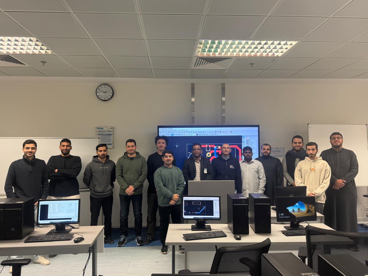
The workshop was organized by the Department of Communications and Networks Engineering, College of Engineering, Prince Sultan University, Saudi Arabia. Dr. Seshagiri Vemparala, a postdoctoral scholar at the Renewable Energy Lab (REL), served as the instructor for the session. The workshop began with an overview of the capabilities and functions of KiCad software, which is used to create printed circuit boards (PCBs). The process of creating schematics and designing PCB layouts was taught to the participants, who also learned about important elements including schematic capture and component libraries. Routing and component placement are among the steps covered in the workshop for both schematic and PCB layout design. Following the theoretical introduction, students and researchers worked hands-on under the instructor's guidance as they experienced the design process. Participants became more comfortable using KiCad to design entire PCBs as a result of this hands-on experience.